
Optical surface roughness: specification, measurement and impact
Optical surface roughness can be understood as the texture of an optical component. It is achieved through, rough grinding / fine grinding / polishing and impacted by surface treatment.
It is provided as a measure of surface variations of only several nm or even ångströms, with two common measuring calculations : RMS & PV.
Roughness is only one part of surface quality, which can additionally be defined by surface figure, waviness, scratch/dig and cleanliness.
Why surface roughness matters
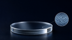
Perfect surface does not exists, even if a surface looks totally “glazed” with raw eyes, there is a level of magnification that will show an uneven surface.
As the surface on an optical component will not be perfect, optical transmission or reflection through this component will be altered, measurement and control of the roughness help to quantify this alteration.
There are two main issues that are addressed with controlling of surface roughness : light scattering and resistance to high power lasers.
The rougher the surface the more light will be scattered and the image quality negatively impacted. Similarly, a rough surface will be a basis of defects on optical components exposed to high power laser beams and therefore limit the amount of energy it can receive without being physically impacted (defined as LIDT – Laser Induced Damage Threshold).
Avoid over-specifying roughness
Better roughness leads to better quality optics, that is true, but it is important to understand why finding the good level of quality is important.
Achieving a lower roughness value will usually need more processing time and may require extra processes likes intermediary and advanced polishing. This leads to longer manufacturing time and more importantly, a very important increase on the optical components costs !
Optical coating will also impact component’s roughness. While users prefers to define finish products roughness, manufacturers prefers to define roughness before coating. Knowing well their polishing equipment, it is easier to guaranty the roughness before the coating and also easier to measure : coating may impact optical roughness measurements of the part.
Indicative roughness values (RMS)
| Polishing level | Indicative OPTICAL surface roughness | Typical use and consideration |
|---|---|---|
| Conventional high-quality polish | Around 20-5 Å RMS (0.5 nm RMS) |
Suitable for many precision optical components. |
| Very fine polish | Around 1–2 Å RMS (0.1–0.2 nm RMS) |
Relevant where lower scatter or improved coating-substrate quality is required, particularly for short-wavelength or high-contrast applications. |
| Superpolish | Below 1 Å RMS (<0.1 nm RMS) |
Used for highly demanding low-scatter, UV, high-power laser and precision-cavity applications. It requires dedicated finishing and metrology. |
Important: These are indicative RMS roughness ranges, not universal acceptance limits. A valid specification must also state the measurement method, scan area or trace length, spatial bandwidth or cut-offs, filtering, form removal, and whether the result applies before or after coating.
Short wavelengths requires closer attention
For comparable surface texture and optical geometry, roughness-driven scatter becomes more significant as wavelength decreases. UV, deep-UV and short-wavelength visible systems therefore often need a better surface finish than a comparable long-wave IR or THz system.
This is a design principle, not a complete specification. Material, refractive index, angle of incidence, coating, clear aperture, detector contrast and permitted stray light also matter. Nor should an IR part automatically receive a relaxed requirement: a low-loss reflector, laser optic or high-contrast detector can still make roughness critical.
RMS and PV explained
Often optical surface roughness is explained in RMS or PV.
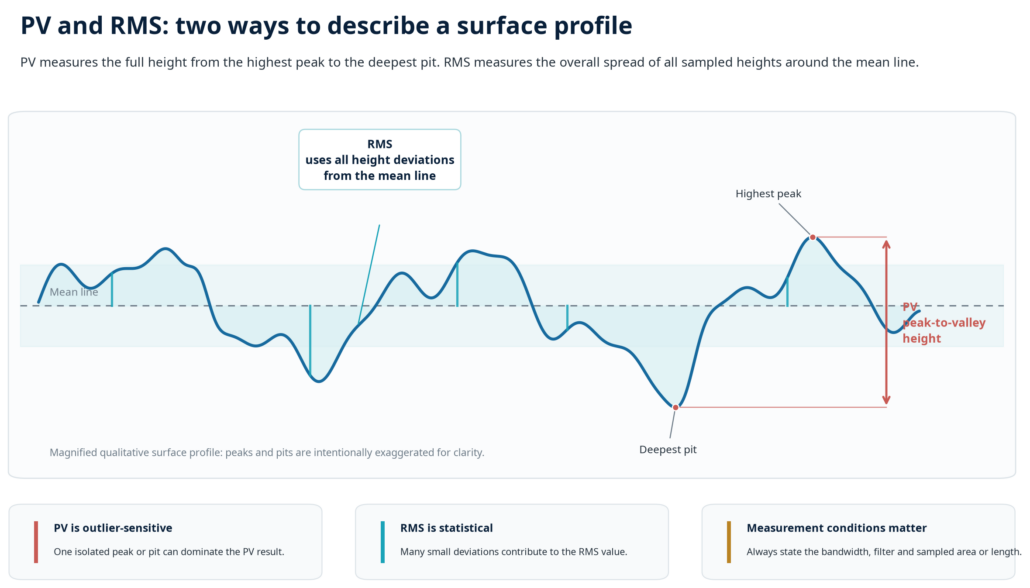
RMS refers to Root Mean Square, which in short is the measurement of the average of all surface imperfection on a given surface.
PV is short for Peak-to-Valley and is defined by the biggest amplitude between pits and peaks on a given surface.
While the former could be understand as an average quality of the surface the later would correspond to the worst default presents on a surface. Both measurements methods are not really measuring the same thing and cannot be calculated back from one another.
More on how to define roughness following ISO 10110.
Measurement methods for optical surface roughness
Find below different measuring methods with their specificity.
| Method | Best use | Points of attention |
|---|---|---|
| Atomic force microscopy (AFM) | Fine microroughness over a small field. | State the scan size and measurement location. AFM data are local, so the measurement must be representative of the relevant clear aperture. |
| White-light / coherence-scanning interferometric profilometry | Non-contact areal texture, waviness and many roughness applications. | Define the objective, lateral resolution, field size, form removal and spatial filtering. These settings determine the spatial band represented by the result. |
| Stylus profilometry | Established 2D surface-profile measurements. | Specify scan direction, tip geometry and filtering. It is a contact method, so it is not ideal for every delicate finished optical surface. |
| Scatterometry | Measuring scattered-light behaviour and correlating it with optical-system performance. | Useful for functional correlation, but it does not replace a defined topographic Rq or Sq measurement when that parameter is the acceptance criterion. |
Other technical information from SINOPTIX


