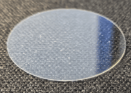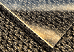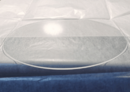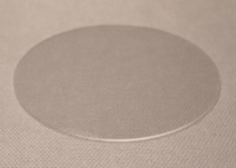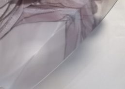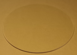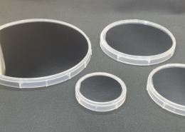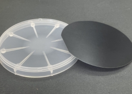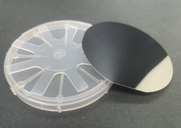

JGS2 wafer
Fused silica thin disc
Part details
Material :
Manufacturing process :
Material cut and polishing
Dimensions:
D150 mm
Thickness 500µm
Shape :
Round disc
Aspect :
Two surfaces are polished, scratch and dig 60/40.
Optical treatment :
None
Usage :
substrate for nano-structured optics