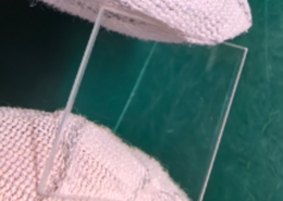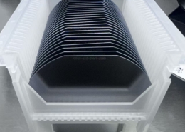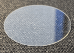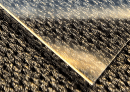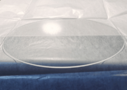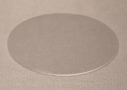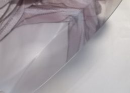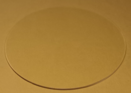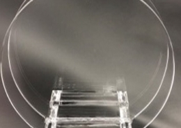

Fused silica wafers
High quality wafer for semiconductors and industry
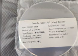
Material : Fused silica (JGS1 & JGS2)
Process : cutting and one face polishing or double face polishing
Dimensions: from diameter 1″ to 20″ ( 25.4mm to 500 mm) +/- 0.05mm
Thickness : 400 µm to 1mm +/- 0.01mm
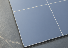
Shape : round with a flat cut. Can be custom diced.
Surface quality : RMS better than 5 nm
TTV : less than 20 µm
Aspect : scratch and ditch 20/10
Usage : semiconductors and industry